
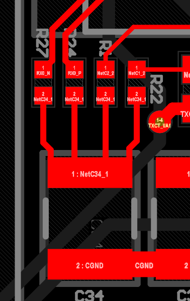
Hello everyone! I’m designing a PCB and I have some doubts about how to connect the 4 resistors at the top to capacitor C34. They are 4 traces, and all of them terminate at the same pad of the capacitor. As I have currently placed them, are they connected correctly? Or should I connect them in a different way?
If it’s for a digital or power-electronics design, you might want to bypass that question entirely and put in a plane/copper pour/copper fill (all synonyms) that encompasses all these pads.
This helps with power dissipation and lowers resistance though has parasitic inductance and capacitance ramifications. It depends on what goes through that net !
On the other hand if this is analog, high frequency, rf or mixed-signal, I would suggest looking at what kind of requirements you have for that net mathematically. You can find the parasitic inductance and capacitance equations (approximations) online quite easily.