
This is apparently what the front looks like.

Socks outside vs inside
Wow even looks like a GPU.
What is it?
Still more reliable than Wayland on nvidia.
also doubles as an electrical fire generator, very versatile
If you are worried about that, then don’t look behind the panel on any computers with a wire wrapped backplane.
The design is very human
Typical spaghetti code
-O2 from the looks of it
Can it play Crysis?
Only gamers will get that joke
-Jensen Huang, Computex, May 29, 2023
It certainly can cause crisis
deleted by creator
Mine almost looks that good
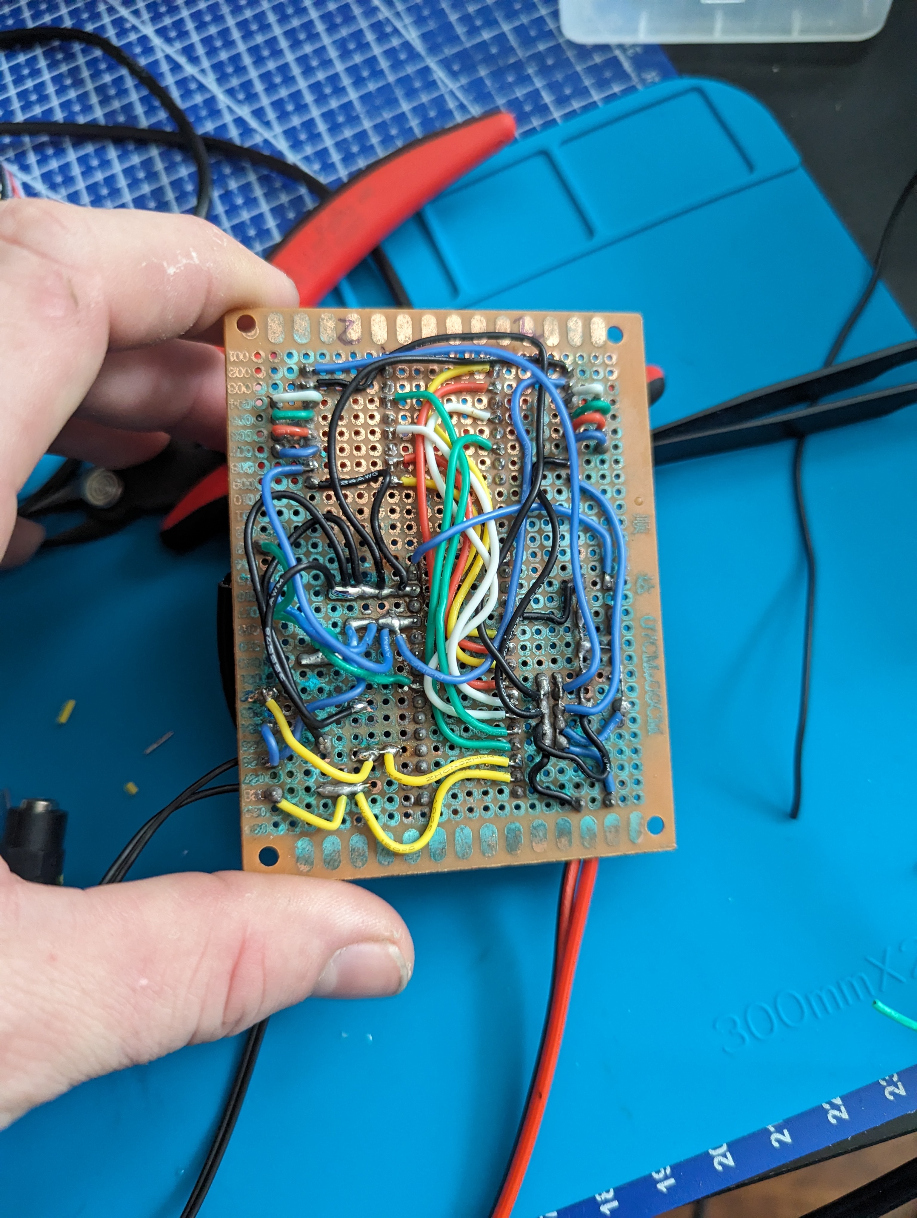
This is a reasonable typical perfboard build by comparison. The above is insanity.
nice
Fire starter 4000
Actually no. Wire wrapping prototypes were made like this. This also looks like an old ISA card as well, from which period this method of prototyping was still in us. It’s also the method in which the Apollo’s guidance computer was made and that one survived a lot harsher conditions than desktop PC, and survived.
If it’s open, looks don’t matter. Also doesn’t matter if the drivers are trash, or if it runs zero games. It’s all fixable trash - that’s the point.
(Also, that’s not a GPU, but it’s the thought that counts)
What am I looking at?
A free and open source GPU compiled by hands
The free and open source comes with the fact it was hand made ? I don’t get it
Would assume that in this case that the gpu was created and assempled using a open blueprint/schematic thats freely available for anyone to see use and modify. Fairly common thing when it comes to stuff like 3d printing where many people freely share their models for others to use.
The joke is in the eye of the beholder, for me it’s funny because you have the buzzwords “free and open source” which means you can implement it however you want and the user here decided “fuck it, I will do it by hand”.
I don’t get it either
It looks like a wire wrapped prototype board of some kind, impossible to tell the purpose from that photo alone though.
I don’t know, maybe it’s not even a GPU
Serious response I agree with Pogo, it looks like a handmade RAM.
Looks like an ISA card to me - might be RAM, but I’m not confident at all
Did you see the pic of the front?
Posted by someone above. https://mander.xyz/pictrs/image/af6db07a-cc89-41f8-840c-3b7d44fb5fb0.jpeg
some pci-e device. but the main chips are probably on the other side of the board.
This looks more like the boards they used in the 60s and 70s in prototyping. I have done such a board myself in my youth. All 40xx and 74LSxx DIL chips and a plain dot board. And a sh-tload of patching wire where I had to remove the isolation paint before I could solder that stuff.
I don’t think you could build a working GPU with that wirewrap technology, the frequncies needed are simply to high.
Haywire. You don’t see that often anymore.
I wonder why
deleted by creator
Surely figuring out home made pcbs is easier than that. Based on things I’ve made that don’t work very well on a breadboard but work better on a pcb, this guy is likely working hard not smart. (I’ve gotten 2 layer homemade pcbs to work before but stopped when pcb fab services became more affordable to hobbyiests)
Are homemade PCBs really that effective? I’d wanted to try my hand at them but never could settle whether it was worth attempting.
My understanding is you make fewer but more replicable mistakes. If you use a wire you have to trace it, keep the length consistent for timing reasons, use very consistent soldering technique, and ultimately you have a hard time tracing issues. With a homemade PCB you generally do get what you ask for in terms of circuitry. Traces are the right length, right thickness, right spacing, and if not then the whole board is similarly impacted, so it is obviously broken or not broken. If you mess up your design then you have a problem, but if you did the process right and you have a valid design then it works.
That all said, homemade PCB is a large time sink and modern PCB manufacture is so cheap and fast it doesn’t make sense to do at home for the most part. You can literally get a complex board faster by ordering it from halfway around the world and having it posted than making it yourself. I would say it is a good learning exercise, not a good manufacturing or prototyping practice.
I mean, if you put in the work to figure all the stuff out when the alternative is to pay $400 for 5 pcbs that take 2 month to get delivered, then yes it is a more viable option. Luckily that’s not the case anymore, but if things so south in China I imagine the only hobbyiest pcbs you can get will be via this method again.
You’ll have to modify or build a heated laminator until it can apply photoresist film perfectly to a sheet of copper clad fr4. The you’ll have to build a uv exposure chamber and a light diffuser (I used a picture frame and a shower curtain). Then put that on a turntable for even light distribution like in a microwave and figure out some way of pressing all the layers together tightly enough so it turns out right and light doesn’t get under the clear stencil you printed the pcb layout to. This will take a lot of trial and error to get right. Then you have to figure all the variables to get it to etch properly through even more trial and error.
Once you have all this stuff figured out, you have to figure out a way to deal with vias. The best way I found was to manually solder a wire or pin for each one and make sure to make them big enough that this can be done by hand. Keep in mind that regular through hole pads won’t be connected on both sides so you need to solder the unused ones for your design to work out.
I wouldn’t go as far as to call this “worth attempting”, especially if you’re trying to make stuff more complicated than an 8 bit computer but for really simple stuff that doesn’t require high precision, super thin traces and lots of vias, it’s not too bad. Simple designs won’t require the same levels of process perfection as trying to make something like an atx motherboard.
With the rise of inexpensive 3d printers, I wonder if milling would be a cheaper option.
We had a PCB mill at the university I went to, a “few” years ago.
Only as effective as your layout skills :)
Check out jlcpcb. Honestly insane what is available to the hobbyist of today
Why does this look like when i first iterate a pcb and need to bodge the hell out of it to make it work.
Judging by the craiglist watermark on the bottom right, it’s probably just a meme listing.
I have stolen it from Chinese website
You switched two wires.


