
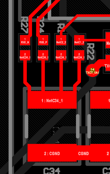
Hello everyone! I’m designing a PCB and I have some doubts about how to connect the 4 resistors at the top to capacitor C34. They are 4 traces, and all of them terminate at the same pad of the capacitor. As I have currently placed them, are they connected correctly? Or should I connect them in a different way?
If it’s for a digital or power-electronics design, you might want to bypass that question entirely and put in a plane/copper pour/copper fill (all synonyms) that encompasses all these pads.
This helps with power dissipation and lowers resistance though has parasitic inductance and capacitance ramifications. It depends on what goes through that net !
On the other hand if this is analog, high frequency, rf or mixed-signal, I would suggest looking at what kind of requirements you have for that net mathematically. You can find the parasitic inductance and capacitance equations (approximations) online quite easily.
As other have mentioned, what you got is fine for most basic applications. If you use a polygon pour you can decrease the resistance of the trace and consolidate it all into one large trace. I also see you using traces for ground, the general rule is if you have the room, make all the unused space on at least one of your layers ground with a polygon pour. This makes connecting ground easier, makes your ground more reliable (decreased resistance) and makes your board less susceptible to external noise
Yeah, they seem fine. A digital application might benefit from making a small plane there, but it’s nothing serious. On the other hand analog applications benefit from star formations, like the one you did. But, it shouldn’t really matter in one case or the other, the leads are too short to make a substantial difference.
Why not just connect all the resistors together with one straight trace, and put on trace between that and the cap. They’ll save copper and make the board cheaper.
Would they really? I made only one PCB so far, but there your price was independent of design. I also don’t think they save a significant amount of copper either way. Would they notice at all? When you etch away the copper from your PCB you would need to measure how much copper your etchant took in and I would imagine that’s not worth the effort. Feel free to correct me if I’m wrong though.
I know of no PCB fab house that prices production on how much copper is etched out of the foil (even though they recycle the dissolved copper afterwards). On the contrary, i usually got the advice of leaving as much copper on the board as I could, as it makes their life easier (and balancing becomes very easy).
It mostly doesn’t matter.
If it’s a high-current, high-frequency, or low-noise circuit then maybe the inductance or resistance of those traces would matter, but they’re very short so probably not.
If you’re mass-producing it, then sometimes the reflow or wave solder process works better if the traces leave the pads in particular ways. You’d talk to your manufacturer about this.
If this is a hobby project, you’re overthinking it; arrange them in a way that pleases you!
