
You can do all sorts of nifty things when you’re designing silicon. Including this abomination.
https://en.wikipedia.org/wiki/Carcinisation
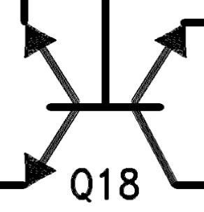
Source: datasheet for LM161, a high speed (20ns delay) moderately high voltage (30V) comparator. I’m going to try and make a discrete version of some bits of it and see how well it works. Maybe not this triple-emitter NPN though, I draw the line at components that require livestock sacrifices.

What is it supposed to do?
I only know what wikipedia tells me about these things, I’ve never played with one. I also have no clue yet what it does in this circuit.
3 emitters and 2 collectors.
There’s just one collector though?
Nope, bottom right and top middle >:DOh my god I’ve forgotten what a base is. This transistor is doing my head in.
This whole circuit is cursed… it looks like for Q19 to be on, the base/collector junction of Q18 must be forward biased - is that even allowed? Does that make the collector a fourth emitter? Or is the whole circuit just made to convey to the reader of the datasheet that they could never ever build this themselves?
I suspect that you need to think of the 3 B->E voltages as inputs (OR’d with each other) and the C->lowestvoltageE path as the output. All of them are operating in linear mode too, I think one of them is a low-gain follower whilst others have a lot more gain. Maybe.
Fascinating, a single transistor that allows multiple logic functions. I can see where that’d be extremely useful in an IC.
I never got to do IC development so it’s cool to me :P