
You can do all sorts of nifty things when you’re designing silicon. Including this abomination.
https://en.wikipedia.org/wiki/Carcinisation
Source: datasheet for LM161, a high speed (20ns delay) moderately high voltage (30V) comparator. I’m going to try and make a discrete version of some bits of it and see how well it works. Maybe not this triple-emitter NPN though, I draw the line at components that require livestock sacrifices.

Interesting way to draw them, but not particularly weird. Bipolar processes don’t really control emitter:collector ratio very well, so gain often varies widely between two transistors even on the same IC. Having extra emitters (or extra collectors) lets the designer match the number of emitters on one transistor to the number of emitters on another, or create ratios between them. That allows for much more accurate gain matching (or gain ratio matching). There are lots of other tricks that can be done in ICs that aren’t really available in discrete components. Camenzind’s book “Designing Analog Chips” goes over quite a few of them.
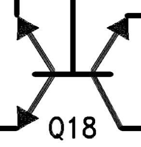
Biblically accurate transistors
What is it supposed to do?
I only know what wikipedia tells me about these things, I’ve never played with one. I also have no clue yet what it does in this circuit.
3 emitters and 2 collectors.
That Wiki page is woefully incomplete, only covering the digital applications (and these days digital stuff is all done with FETs, not BJTs). Camenzind’s Designing Analog Chips has quite a bit more info.
It’s hard to control the exact area of the emitter diffusion in a BJT. Think of how an NPN transistor is made on an IC: there’s some substrate that the collector gets connected to, then an area is masked off & the unmasked area is doped enough to make it a P-type silicon region. That doping process will have some variation in depth & the masking is never perfect, some will diffuse a bit past the edges of the mask, or not enough will diffuse in. Then another mask layer is applied, and N-dopant is added in the open space to form the emitter. That’s also imperfect, on top of an already imperfect base. So the exact gain of transistors isn’t well-controlled, even for a very well-controlled collector voltage.
Instead, IC makers can dope multiple smaller emitters in a bigger base region. Smaller doped regions are easier to control (less time for over-diffusion of the dopant) and having a bunch of them has an extra advantage: you can match the ratio of collectors to emitters from one transistor to the ratio of collectors to emitters of another, and variations in the area of any individual emitter will be a much smaller percentage of the total error since the errors of the different emitters will tend to cancel out.
Also, the high-current capability of a BJT is controlled by the emitter length, not the emitter area. Splitting an emitter into long strips can increase how much current a transistor can handle.
Similar things apply to the collector.
For SPICE modeling or building discrete versions of ICs, use multiple transistors in parallel.
Fascinating, a single transistor that allows multiple logic functions. I can see where that’d be extremely useful in an IC.
I never got to do IC development so it’s cool to me :P
There’s just one collector though?
Nope, bottom right and top middle >:DOh my god I’ve forgotten what a base is. This transistor is doing my head in.
This whole circuit is cursed… it looks like for Q19 to be on, the base/collector junction of Q18 must be forward biased - is that even allowed? Does that make the collector a fourth emitter? Or is the whole circuit just made to convey to the reader of the datasheet that they could never ever build this themselves?
I suspect that you need to think of the 3 B->E voltages as inputs (OR’d with each other) and the C->lowestvoltageE path as the output. All of them are operating in linear mode too, I think one of them is a low-gain follower whilst others have a lot more gain. Maybe.
How can it be, it’s emitting more than it’s collecting. Unnatural.
I don’t want my children influenced by this. “Dad why does your transistor only have 3 legs?”. And I had only just rid the house of dual-gate mosfets too!
_Cross-section.svg)